TPU architecture
Tensor Processing Units (TPUs) are application specific integrated circuits (ASICs) designed by Google to accelerate machine learning workloads. Cloud TPU is a Google Cloud service that makes TPUs available as a scalable resource.
TPUs are designed to perform matrix operations quickly making them ideal for machine learning workloads. You can run machine learning workloads on TPUs using frameworks such as Pytorch and JAX.
How do TPUs work?
To understand how TPUs work, it helps to understand how other accelerators address the computational challenges of training ML models.
How a CPU works
A CPU is a general-purpose processor based on the von Neumann architecture. That means a CPU works with software and memory like this:
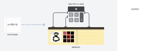
The greatest benefit of CPUs is their flexibility. You can load any kind of software on a CPU for many different types of applications. For example, you can use a CPU for word processing on a PC, controlling rocket engines, executing bank transactions, or classifying images with a neural network.
A CPU loads values from memory, performs a calculation on the values and stores the result back in memory for every calculation. Memory access is slow when compared to the calculation speed and can limit the total throughput of CPUs. This is often referred to as the von Neumann bottleneck.
How a GPU works
To gain higher throughput, GPUs contain thousands of Arithmetic Logic Units (ALUs) in a single processor. A modern GPU usually contains between 2,500–5,000 ALUs. The large number of processors means you can execute thousands of multiplications and additions simultaneously.
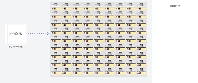
This GPU architecture works well on applications with massive parallelism, such as matrix operations in a neural network. In fact, on a typical training workload for deep learning, a GPU can provide an order of magnitude higher throughput than a CPU.
But, the GPU is still a general-purpose processor that has to support many different applications and software. Therefore, GPUs have the same problem as CPUs. For every calculation in the thousands of ALUs, a GPU must access registers or shared memory to read operands and store the intermediate calculation results.
How a TPU works
Google designed Cloud TPUs as a matrix processor specialized for neural network workloads. TPUs can't run word processors, control rocket engines, or execute bank transactions, but they can handle massive matrix operations used in neural networks at fast speeds.
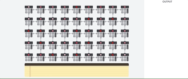
The primary task for TPUs is matrix processing, which is a combination of multiply and accumulate operations. TPUs contain thousands of multiply-accumulators that are directly connected to each other to form a large physical matrix. This is called a systolic array architecture. Cloud TPU v3, contain two systolic arrays of 128 x 128 ALUs, on a single processor.
The TPU host streams data into an infeed queue. The TPU loads data from the infeed queue and stores them in HBM memory. When the computation is completed, the TPU loads the results into the outfeed queue. The TPU host then reads the results from the outfeed queue and stores them in the host's memory.
To perform the matrix operations, the TPU loads the parameters from HBM memory into the Matrix Multiplication Unit (MXU).
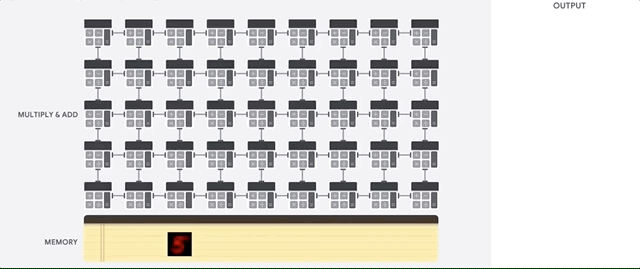
Then, the TPU loads data from HBM memory. As each multiplication is executed, the result is passed to the next multiply-accumulator. The output is the summation of all multiplication results between the data and parameters. No memory access is required during the matrix multiplication process.
As a result, TPUs can achieve a high-computational throughput on neural network calculations.
TPU system architecture
The following sections describe the key concepts of a TPU system. For more information about common machine learning terms, see Machine Learning Glossary.
If you are new to Cloud TPU, check out the TPU documentation home page.
TPU chip
A TPU chip contains one or more TensorCores. The number of TensorCores depends on the version of the TPU chip. Each TensorCore consists of one or more matrix-multiply units (MXUs), a vector unit, and a scalar unit. For more information about TensorCores, see A Domain-Specific Supercomputer for Training Deep Neural Networks.
An MXU is composed of either 256 x 256 (TPU v6e) or 128 x 128 (TPU versions prior to v6e) multiply-accumulators in a systolic array. MXUs provide the bulk of the compute power in a TensorCore. Each MXU is capable of performing 16K multiply-accumulate operations per cycle. All multiplies take bfloat16 inputs, but all accumulations are performed in FP32 number format.
The vector unit is used for general computation such as activations and softmax. The scalar unit is used for control flow, calculating memory addresses, and other maintenance operations.
TPU Pod
A TPU Pod is a contiguous set of TPUs grouped together over a specialized network. The number of TPU chips in a TPU Pod is dependent on the TPU version.
Slice
A slice is a collection of chips all located inside the same TPU Pod connected by high-speed inter chip interconnects (ICI). Slices are described in terms of chips or TensorCores, depending on the TPU version.
Chip shape and chip topology also refer to slice shapes.
Multislice versus single slice
Multislice is a group of slices, extending TPU connectivity beyond the inter-chip interconnect (ICI) connections and leveraging the data-center network (DCN) for transmitting data beyond a slice. Data within each slice is still transmitted by ICI. Using this hybrid connectivity, Multislice enables parallelism across slices and lets you use a greater number of TPU cores for a single job than what a single slice can accommodate.
TPUs can be used to run a job either on a single slice or multiple slices. Refer to the Multislice introduction for more details.
TPU cube
A 4x4x4 topology of interconnected TPU chips. This is only applicable to 3D topologies (beginning with TPU v4).
SparseCore
SparseCores are dataflow processors that accelerate models using sparse operations. A primary use case is accelerating recommendation models, which rely heavily on embeddings. v5p includes four SparseCores per chip, and v6e includes two SparseCores per chip. For an in-depth explanation on how SparseCores can be used, see A deep dive into SparseCore for Large Embedding Models (LEM). You control how the XLA compiler uses SparseCores using XLA flags. For more information, see: TPU XLA flags.
Cloud TPU ICI resiliency
ICI resiliency helps improve fault tolerance of optical links and optical circuit switches (OCS) that connect TPUs between cubes. (ICI connections within a cube use copper links that are not impacted). ICI resiliency allows ICI connections to be routed around OCS and optical ICI faults. As a result, it improves the scheduling availability of TPU slices, with the trade-off of temporary degradation in ICI performance.
For Cloud TPU v4 and v5p, ICI resiliency is enabled by default slices that are one cube or larger, for example:
- v5p-128 when specifying accelerator type
- 4x4x4 when specifying accelerator config
TPU versions
The exact architecture of a TPU chip depends on the TPU version that you use. Each TPU version also supports different slice sizes and configurations. For more information about the system architecture and supported configurations, see the following pages:
TPU cloud architecture
Google Cloud makes TPUs available as compute resources through TPU VMs. You can directly use TPU VMs for your workloads or use them through Google Kubernetes Engine or Vertex AI. The following sections describe key components of the TPU cloud architecture.
TPU VM architecture
The TPU VM architecture lets you directly connect to the VM physically connected to the TPU device using SSH. A TPU VM, also known as a worker, is a virtual machine running Linux that has access to the underlying TPUs. You have root access to the VM, so you can run arbitrary code. You can access compiler and runtime debug logs and error messages.
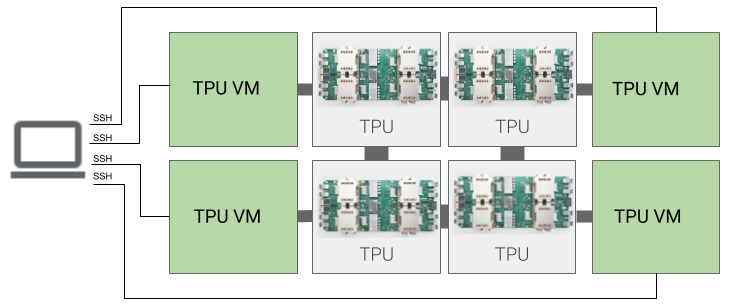
Single host, multi host, and sub host
A TPU host is a VM that runs on a physical computer connected to TPU hardware. TPU workloads can use one or more host.
A single-host workload is limited to one TPU VM. A multi-host workload distributes training across multiple TPU VMs. A sub-host workload doesn't use all of the chips on a TPU VM.
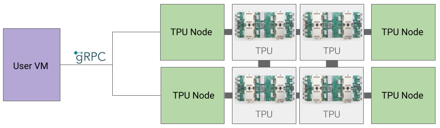
TPU Node architecture (deprecated)
The TPU Node architecture consists of a user VM that communicates with the TPU host over gRPC. When using this architecture, you cannot directly access the TPU Host, making it difficult to debug training and TPU errors.
Moving from TPU Node to TPU VM architecture
If you have TPUs using the TPU Node architecture, use the following steps to identify, delete, and re-provision them as TPU VMs.
Go to the TPUs page:
Locate your TPU and its architecture under the Architecture heading. If the architecture is "TPU VM", you don't need to take any action. If the architecture is "TPU Node" you need to delete and re-provision the TPU.
Delete and re-provision the TPU.
See Managing TPUs for instructions on deleting and re-provisioning TPUs.