Lighting the way: How ASML revived Moore's Law and remade chipmaking

Matt AV Chaban
Senior Editor
Declaring the death of Moore’s Law has become something of a popular pastime in tech circles, based on the assumption that chips will have to stop doubling in power every two years because there has to be a limit to how many transistors can fit on them. Right?
And yet, chipmakers continue to defy expectations — and to some degree, physics. Beyond the boundaries of what previously thought possible, computer chips keep getting smaller and more powerful with the help of new technologies, many of which live on the cloud.
Artificial intelligence has helped researchers design better chips. High-performance computing lets scientists model those designs faster than ever. Big data and analytics allow for the better organization of information and faster test cycles. The end of Moore’s Law may well be on the horizon, but that hasn’t stopped the semiconductor industry from using every cutting-edge technology at its disposal to push that seeming inevitability further down the road.
One major reason why Moore’s Law remains alive and well has been the work of Dutch firm ASML.
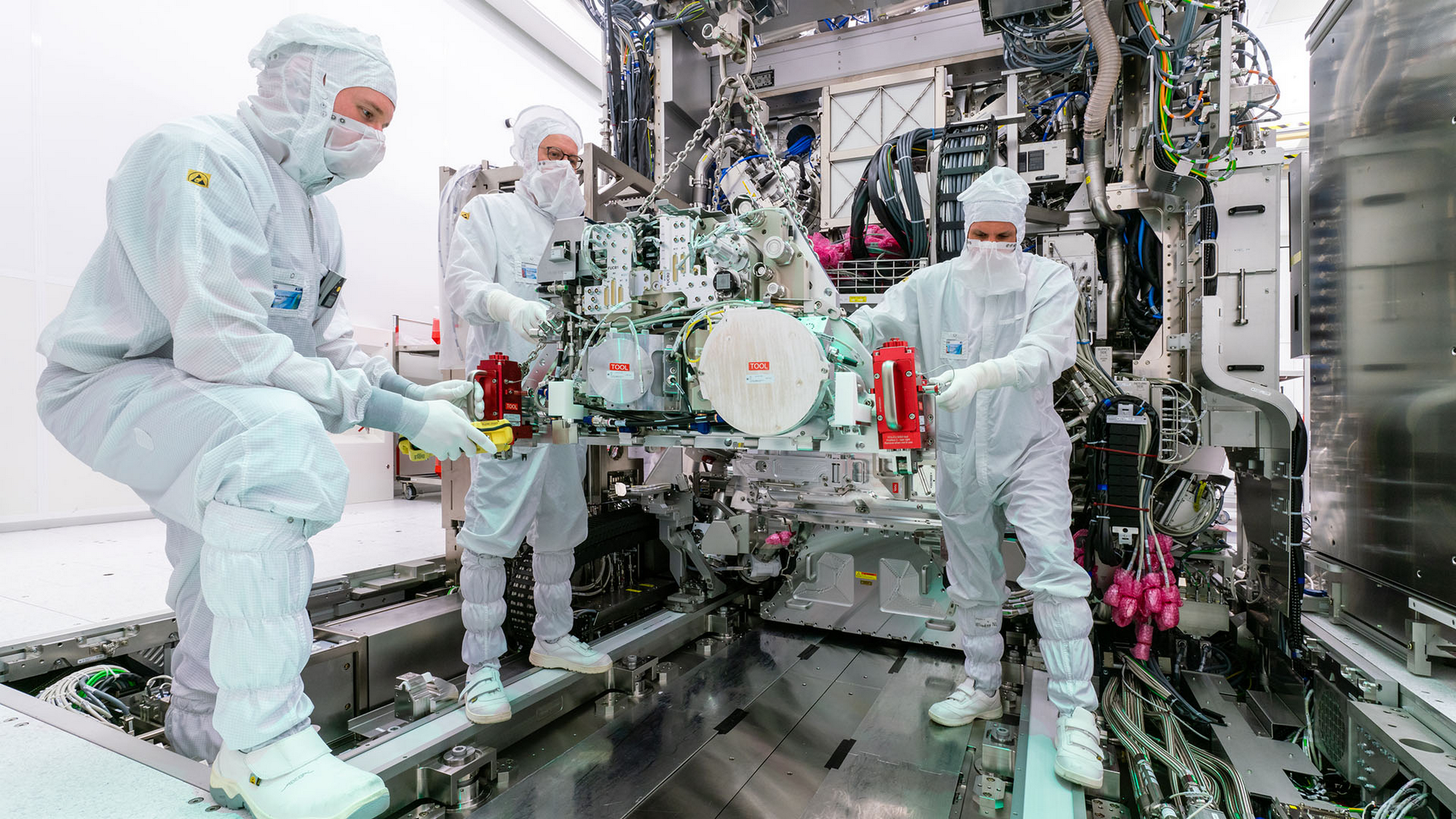
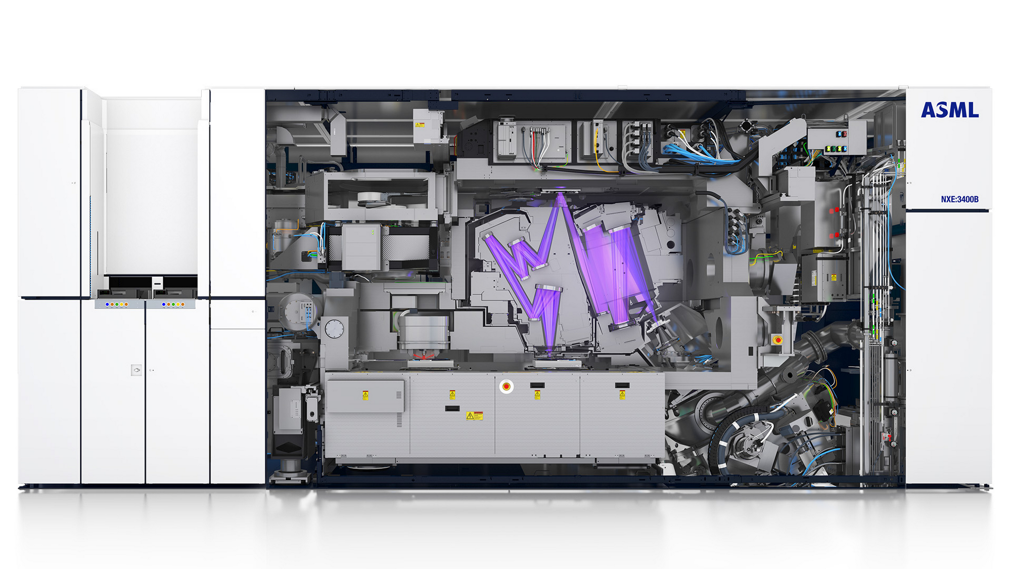
The company builds photolithography machines, software, and solutions that allow manufacturers to make ever smaller, more efficient, and powerful computer chips. After 20 arduous years of research and development, ASML had a major breakthrough in 2017 on the machines that enable high-end chip manufacturing.
The result: a photolithography machine that uses wavelengths of extreme ultraviolet (EUV) radiation to make features in microchips as small as 13 nanometers. MIT Technology Review called it “the machine that saved Moore’s Law.”
The EUV machine took two decades of R&D, with industry experts openly doubting whether it would ever come to fruition. But through sheer determination, billions of dollars of investment, and some clever cloud-based tools, ASML finally broke through and is currently the only vendor in the world that offers the solution. The company has since been selling its machines to the top chipmakers, including Samsung, Intel, and TSMC — at a crucial time, no less, given the chip shortages and related geopolitical tensions.

Arnaud Hubaux, product cluster manager at ASML, borrowed a story from one of those customers on the latest episode of the Transformation Debrief video series to highlight just how focused the mission for the EUV machines has been: “I think Mark Liu, the chairman of TSMC, phrased it beautifully. He said, ‘The semiconductor industry for the past 50 years has been working in a tunnel.’ Everyone knew exactly where to go. The end was clear, the goal was clear: to shrink transistors and make them smaller. So everything with ASML was focused on that.”
The EUV machine, along with all of ASML’s other products and services, need to be extraordinarily precise. Semiconductor manufacturing requires a very complicated set of equipment that possess speed, efficiency, and accuracy to the smallest degrees. As much as the company has produced stunning innovation to build its EUV solution, it has also broken new ground with testing and measurement.
To advance many of these breakthroughs, ASML has utilized cloud technology and artificial intelligence to make its processes more efficient, speed up its testing and quality assurance cycles, and identify potential errors before they become serious problems. Even with the less cutting edge machines, like the “deep ultraviolet,” or DUV, machines that preceded EUV, the horsepower of the cloud is helping drive these enhancements and improvements, too.
“We had to make better sensors, better actuators, better light sources,” Hubaux said. “What you see now happening is that those machines are good enough, though. And, especially with another chip shortage, you want to optimize the utilization of those machines.”
That’s where the programs building and operating the machines are becoming as important as the machines themselves. “The optimization of those machines is something that you typically drive with software,” Hubaux said, “and that requires massive data processing.”
Massive data on the smallest scales
Hubaux has previously described ASML’s photolithography machines as “engineering a race car for an F1 driver.” Considering the miniscule scale at which chipmaking takes place, there is little to no margin for error. Everything in a photolithography machine needs to be calibrated down to the nanometer. With such a complicated machine, that kind of analysis and calibration creates a lot of data.
“We realized that our local environment, the environment we had on-prem, was not sufficient to drive the analysis we wanted to do, the product we wanted to build,” Hubaux said of ASML’s decision to migrate to Google Cloud several years ago.
ASML worked with Google Cloud partner Rackspace and machine learning specialist ML6 to build the architecture and artificial intelligence models needed to ingest, process, and parse in near real-time.


“We noticed quickly after six months that the performance of the team improved 10 times,” Hubaux said. “The overall cycle of application development improves significantly.”
The primary motivation to migrate to the cloud and institute machine learning models that could help analyze its massive amounts of data was so AMSL could speed up the time with which it brought products to market. In the cloud, ASML engineers could run more tests and understand the results more quickly, accelerating R&D and production.
“The main driver was time to market,” Hubaux said. “We needed to be faster at releasing our solutions and also improving the quality of our solutions.”
On that front, the team more than succeeded, achieving a 40% improvement on time-to-market speeds.
Creating a competitive edge with cloud and AI
Hubaux notes that the cloud has yet to be widely adopted in the chipmaking industry. It’s a sector where intellectual property is guarded like a dragon’s lair full of gold and the manufacturing processes of extremely complex machines do not lend themselves to easy data gathering from sensors with an internet connection. All that being said, ASML has found that it can apply the cloud and machine learning to a variety of other properties within its operation to increase speed and efficiency.
“I expect that in the coming two to three years, there will be as slow a shift towards the cloud for the non-critical processes,” Hubaux said. “Those non-critical processes include diagnostics and monitoring that tend to be very data intensive.
ASML’s engineers welcomed the cloud, which allowed them to offload tasks that previously had to be performed manually.
“The engineers who had to deliver the solutions were super excited to onboard to the cloud, because for them, they could use state-of-the-art technology,” Hubaux said. “Everything they had had to maintain themselves — like updating tools, maintaining connections, securing the environment — was something that was very labor intensive, and all of a sudden all those hurdles were removed, so they could really focus on delivering what they were supposed to deliver, which is model good software.”

The chip manufacturing industry is one in which everything that happens needs to be explainable, down to the tiniest detail. ASML’s clients need to understand everything about how the machine works — its sensors, diagnostics, monitoring, and maintenance — to keep pumping out chips. As such, neural network-based artificial intelligence can be a difficult sell because of the “black-box” nature of the algorithms.
In other words, chipmakers could have been hesitant to use ASML’s machines unless they know exactly the outcomes any AI might deliver.
“When you are talking about high-volume manufacturing,” Hubaux said, “those machines have been tuned so much that any change to those machines could lead to a potential half-life down the line. That could really stop production, and cost customers millions. For that kind of scenario, machine learning is a thing not very widely adopted yet because of this black-box effect.”
Quality assurance, and assuring continued chip innovation
One area where ASML has seen success with AI is in quality assurance. Chips are very small and thus nearly impossible to manually inspect. But the team was able to train AI to quickly look for defects with low-resolution images of chips by training inspection models.
“This is where AI kicked in because we still used a physics model to classify a picture as good, bad, a defect, or a non-defect based on physics,” Hubaux said. “We used AI that we trained on high-resolution images to recognize low resolution images, filling in the blanks with the physics model.”
“So that's where AI is actually enhancing the capability of the hardware, to make this kind of virtual extension of the hardware that is improving the quality for predictions,” he continued. “And it’s also the big benefit for the customer, making it cheaper.”
Ultimately, ASML has threaded an extraordinary needle.
It has built one of the most advanced machines in history with its EUV photolithography equipment, driving the next generation of chips. It has also been able to take those advances and increase the company’s efficiency, optimizing its processes through the cloud and artificial intelligence in an industry where those solutions are often difficult to implement.
In a way, it’s a story as old as Moore’s Law, if not much older. Technology drives advancing technology, which advances new technology, which advances new technology . . . ever onward. And ASML is at the heart of these advances, driving its business to advance others, and setting itself up for the next leap forward . . . ever onward.


