Synopsys helps semiconductor designers accelerate chip design and development on Google Cloud

Jyotsna Repaka
Customer Engineer Lead
Mark Mims
Solutions Architect
Google Cloud and Synopsys Inc are partnering to help semiconductor companies drive Electronic Design Automation (EDA) innovation in the cloud to accelerate time to market, and lower costs across the entire semiconductor product life cycle. Synopsys is the industry’s largest provider of EDA technology used in the design and verification of integrated circuits, or semiconductor chips. Bringing Synopsys technology onto Google Cloud enables customers to benefit from scalable cloud bursting and complementary licensing models to help them quickly deploy and scale Synopsys’ EDA tools. Semiconductor companies can significantly accelerate chip design and production, increase designer productivity, and empower innovation in power-performance-area optimization.
Google Cloud Platform has enabled high performance computing workloads, such as those used by today’s semiconductor chip designers, to deliver exceptionally fast results and reduce prototyping from years to months. Google Cloud’s HPC services have delivered highly scalable solutions across multiple industries - from scientific research, to autonomous vehicle testing and simulation.
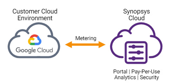
EDA software is a large consumer of high performance computing capacity in the cloud. With the release of Synopsys Cloud bring-your-own-cloud (BYOC) solution on Google Cloud, chip designers can now scale their Google Cloud infrastructure with Synopsys’s leading EDA tools under the flexible FlexEDA pay-per-use model and access unlimited EDA software license availability on-demand by the hour or minute.
The Synopsys Cloud BYOC deployment architecture on Google Cloud is enabled through their unique cloud metering service which uses Google Cloud regional MIGs (Managed Instance Groups) for autoscaling and multi-zone deployment. This enables the service to scale up to meet customer workload demands and scale down to optimize costs. Secrets used by Synopsys Cloud are securely stored in Google Secret Manager and usage data is encrypted using Google Cloud key management, providing customers with a highly secure design environment.
Synopsys Cloud also leverages Google Cloud's Ops Agent and Operations Suite Dashboards are used to show metric data, alerting policies, and log entries, providing customers with detailed analytics visibility to make better chip design project lifecycle management decisions. The Synopsys Cloud BYOC solution has been validated with EDA workloads scaling out to thousands of cores on Google Cloud, using Google Filestore network file storage during validation to provide the highest throughput performance.


Vikram Bhatia, Head, Synopsys Cloud Product Management, Synopsys said, “With the release of Synopsys Cloud BYOC solution on Google Cloud, we are transforming the way our mutual semiconductor customers can design the chips of the future. Google Cloud has been leading the innovation wave for semiconductors in the cloud and we are excited about being an early adopter in leveraging those innovations for our unique EDA offerings on the cloud.” Customers can evaluate a full featured Synopsys Cloud BYOC environment on Google Cloud for free by signing up at: synopsys.com/cloud.
“Combined with GCP’s unique platform services for AI, security, and shared storage, the Synopsys Cloud BYOC solution creates a compelling package for semiconductor designers who will create the next generation of chips for the world’s insatiable needs” says Simon Floyd, Industry Director, Manufacturing & Transportation, Google Cloud.
Google Cloud provides everything you need, including free Google Cloud credits to get you up and running. Click here to learn more about Semiconductors on Google Cloud.


