Google chip design team benefits from move to Google Cloud
Lital Levy
Product Marketing Manager
Bukola Ayodele
Developer Advocate
Editor’s note: All companies can wrestle with a cloud migration, even Google. That’s why within Google Cloud, we have a team called Alphabet Cloud whose mission is to assist any Alphabet team with a safe, frictionless journey to Google Cloud. Some of these internal customers include DeepMind, Vertex AI, Waze, and, today’s example, Google’s chip development infrastructure team. This team’s migration to Google Cloud highlights how removing the limitations of on-premises infrastructure can unleash a team’s potential, and empower developers to innovate — in this case, the revolutionary chipsets powering tomorrow’s cloud infrastructure.
Many people know Google for its search tools, software services like Google Maps, and Android, but did you know that Google also develops its own dedicated hardware? Google designs and creates chips in house that are used for machine learning supercomputers, Pixel phones, networking infrastructure, and even video accelerators for YouTube.

Before Google Cloud
The chip development infrastructure team was born in a data center, on a single rack of computers, but quickly grew into dozens of racks and hundreds of servers as workloads grew more complex. As projects began to mount, so did the implementation challenges, with hardware costs doubling annually, and each new initiative requiring new engineers and infrastructure. When the team was prioritizing hiring engineers simply to manage and optimize legacy machines, they knew they were losing sight of their core focus: growth and innovation.
Before migrating entirely to Google Cloud, the team explored a hybrid solution using Google’s internal software design environment, and some Electronic Design Automation (EDA) workloads sent into Google Cloud. While the approach was reliable in the short-term, delays in transferring workloads for analysis would leave engineers waiting around for results. The added burden of having two desktops running concurrently, one for their design environment and one for their results in Google Cloud, led to a rethink.
Believing there was a better solution that would minimize the challenges of this hybrid approach, the chip development infrastructure team reached out to the Alphabet Cloud team. The Alphabet Cloud team sits within Google Cloud and is responsible for helping teams across Alphabet accelerate their adoption of Google Cloud's unique offerings to drive faster development and scale, just like a customer's platform team would.
Transition to using Google Cloud
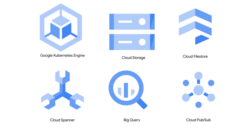
The chip development infrastructure team worked in collaboration with Alphabet Cloud on a full migration to Google Cloud. After a thorough evaluation of the current infrastructure, their analysis uncovered that the following Google Cloud tools would be most beneficial: Google Kubernetes Engine (GKE) for their containers, and for data, Cloud Storage, Filestore, Cloud Spanner, Big Query, and Pub/Sub.

The business benefits of this move to Google Cloud were significant. The first benefit was the elasticity of the cloud, specifically the ability to grow on demand and request resources quickly and efficiently. The lead times to provision new specialized compute infrastructure went from six months to just a few days. Another benefit the team received was a reduction in operational costs, which meant they could now manage a much bigger footprint. With Google Cloud, infrastructure bugs could be identified and resolved within hours. The team could also innovate faster because it was spending less time on data center maintenance.
Outside of resource management benefits, the team was able to leverage Google Cloud’s AI and ML capabilities to design more efficient chips. They leveraged various ML algorithms, readily available in Google Cloud to efficiently navigate large search spaces and apply unique optimizations at various stages of chip design. This resulted in a shortened chip design process, reduced time-to-market, expanded product areas for ML accelerators, and improved efficiency.
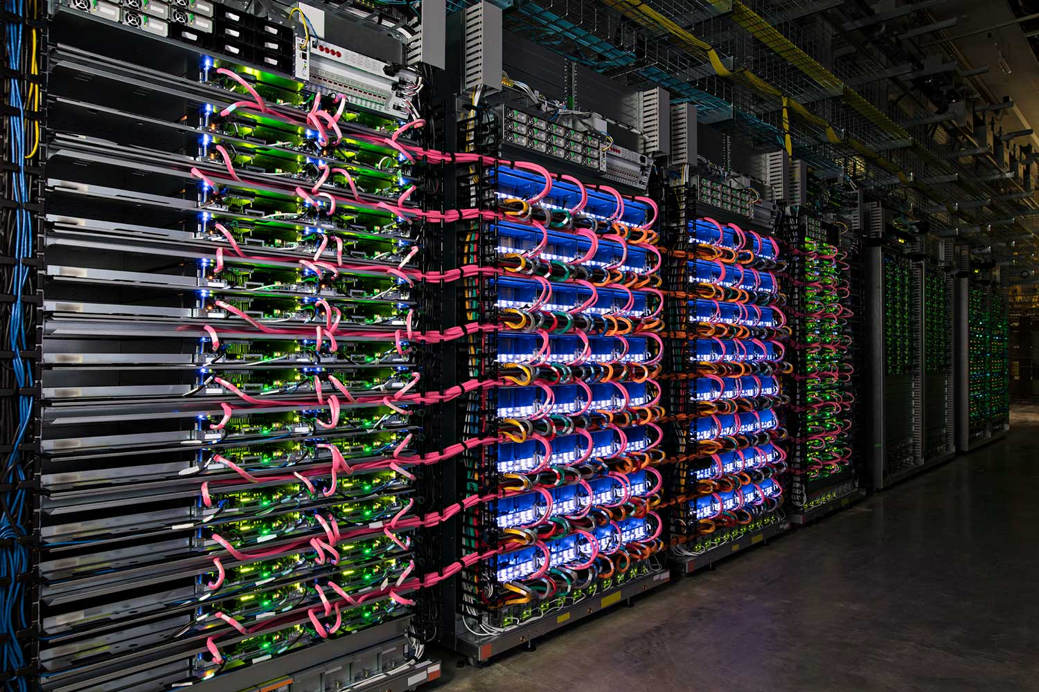
The chip design team has launched full designs built using Google Cloud, including the last two generations of TPUs and YouTube’s video accelerator program, Argos VCU. Without the size limitations of a physical datacenter, chip designers were able to run more jobs to weed out bugs. Since moving to Google Cloud, the team increased daily job submissions by 170% over the past year while maintaining a flat scheduling latency. The workload is supported across 250+ GKE clusters spanning multiple Google Cloud regions. The platform also mediates access to EDA tool licenses needed to run jobs on Google Cloud.

Looking to the future
With Google Cloud’s AI and data capabilities, the chip development infrastructure team can anticipate resource usage and use less compute resources as a result. With access to all metadata, enabled by the massive storage available in Google Cloud, the chip design team can optimize the data storage type to enable the fastest medium for the jobs. Chip design and development will now only continue to improve in its efficiency. In the future, the chip development infrastructure team plans to open source parts of its process, specifically its Bazel build rules and regression systems, so other chip manufacturers can benefit from the approach they used with Google Cloud.
To learn more about how other companies are designing chips using Google Cloud, start here.
