Never miss a tapeout: Faster chip design with Google Cloud
Sashi Obilisetty
Chief Architect, Silicon Solutions
Mark Mims
Solutions Architect
Cloud offers a proven way to accelerate end-to-end chip design flows. In a previous blog, we demonstrated the inherent elasticity of the cloud, showcasing how front-end simulation workloads can scale with access to more compute resources. Another benefit of the cloud is access to a powerful, modern and global infrastructure. On-prem environments do a fantastic job of meeting sustained demand but Electronic Design Automation (EDA) tooling upgrades happen much more frequently (every six to nine months) than typical on-prem data center infrastructure upgrades (every three to five years).
What this means is that your EDA tool can provide much better performance if given access to the right infrastructure. This is especially useful in certain phases of the design process.
Take for example, a physical verification workload. Physical verification is typically the last step in the chip design process. In simplified terms, the process consists of verifying design rule checks (or DRCs) against the process design kit (PDK) provided by the foundry. It ensures that the layout produced from the physical synthesis process is ready for handoff to a foundry (in-house or otherwise) for manufacturing. Physical verification workloads tend to require machines with large memories (1TB+) for advanced nodes. Having access to such compute resources enables more physical verification to run in parallel, increasing your confidence in the design that is being taped out (i.e., sent to manufacturing).
At the other end of the spectrum are functional verification workloads. Unlike the physical verification process described above, functional verification is normally performed in the early stages of design and typically requires machines with much less memory. Furthermore, functional verification (dynamic verification in particular) accounts for the most time (translating directly to the availability of compute) in the design cycle. Verifying faster, an ambition for most design teams, is often tied to availability of right-sized compute resources.
The intermittent and varied infrastructure requirements for verification (both functional and physical) can be a problem for organizations with on-prem data centers. On-prem data centers are optimized for maximizing utilization—this does not directly address access to right-sized compute to deliver the best tool performance. Even if the IT and Computer Aided Design (CAD) departments choose to provision additional suitable hardware, the process of provisioning, acquiring and setting up new hardware on-prem typically takes months for even the most modern organizations. A “hybrid” flow that enables use of on-prem clusters most of the time, but provides seamless access to cloud resources as needed would be ideal.
Hybrid chip design in action
You can improve a typical verification workflow simply by utilizing a hybrid environment that provides instantaneous access to better compute. To illustrate, we chose a front-end simulation workflow, and designed an environment that replicates on-prem and cloud clusters. We also took a few more liberties to simplify the environment (described below). The simplified setup is provided in a GitHub repository for you to try out.
In any hybrid chip design flow, there are a few key considerations:
- Connectivity between on-prem infrastructure and the cloud: Establishing connectivity to the cloud is one of the most foundational aspects of the flow. Over the years, this has also become a very well-understood field, and secure, high availability connectivity is a reality in most setups.
In our tutorial, we represent both on-prem and cloud clusters as two different networks in the cloud where all traffic is allowed to pass between these networks. While this is not a real-world network configuration, it is sufficient to demonstrate the basic connectivity model. - Connection to license server: Most chip design flows utilize tools from EDA vendors. Such tools are typically licensed, and you need a license server with valid licenses to operate the tool. License servers may remain on-prem in the hybrid flow, so long as latency to the license server is acceptable. You can also install license servers in the cloud on a Compute Engine VM (particularly sole-tenant nodes) for lower latency. Check with your EDA vendors to understand if you can rehost your license services in the cloud.
In our tutorial, we use an open source tool (Icarus Verilog Simulator) and therefore, do not need a license server. - Identifying data sources and syncing data: There are three important aspects in running EDA jobs: the EDA tools themselves, the infrastructure where the tools run, and the data sources for the tool run. Tools don’t change much, and can be installed on cloud infrastructure. Data sources, on the other hand, are primarily created on-prem and updated regularly. These could be SystemVerilog files that describe the design, the testbenches or the layout files. It is important to sync data between on-prem and cloud to maintain parity. Furthermore, in production environments, it’s also important to maintain a high-performance syncing mechanism.
In our tutorial, we create a file system hierarchy in the cloud that is similar to one you’d find on-prem. We transfer the latest input files before invoking the tool. - Workload scheduler configuration and job submission transparency: Most environments that leverage batch jobs use job schedulers to access a compute farm. An ideal environment finds the balance between cost and performance, and builds parameters in the system to enable predictive (and prescriptive) wrappers to job schedulers (see picture below).
In our tutorial, we use the open-source SLURM job scheduler and an auto-scaling cluster. For simplicity, the tutorial does not include a job submission agent.
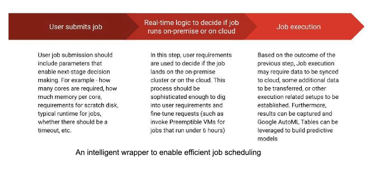

Other cloud-native batch processing environments such as Kubernetes can also provide further options for workload management.
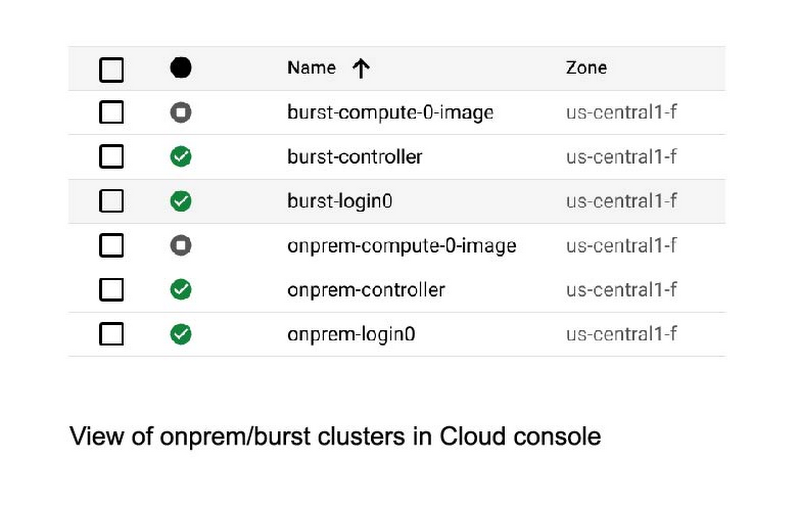
Our on-prem network is called ‘onprem’ and the cloud cluster is called ‘burst’. Characteristics of the on-prem and burst clusters are specified below:


Once set up, we ran the OpenPiton regression for single and two-tile configurations. You can see the results below:
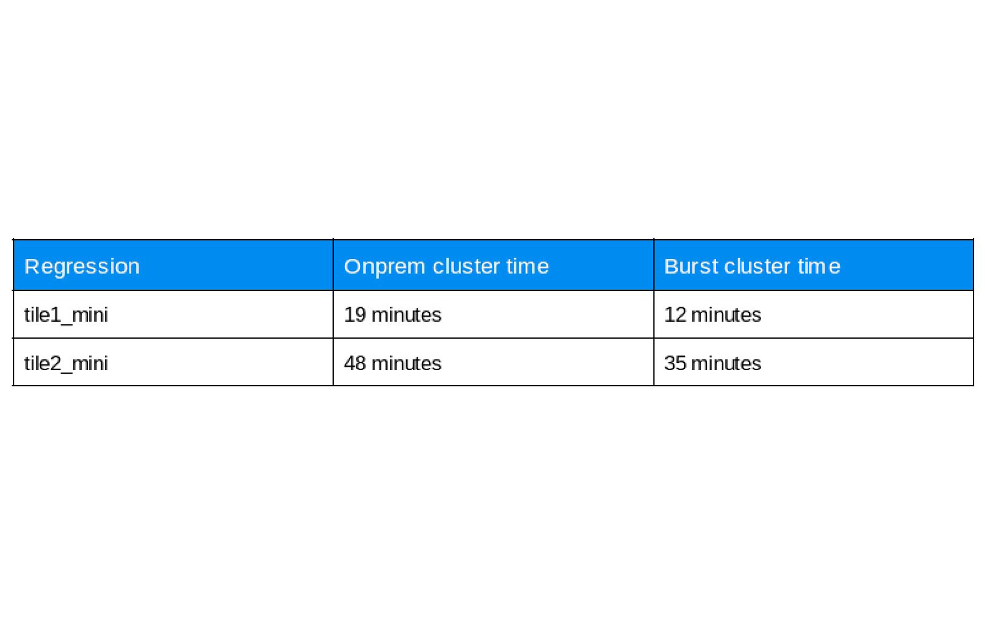

Regressions run on “burst” clusters were on average 30% faster than on “onprem”, delivering faster verification sign-off and physical verification turnaround times. You can find details about the commands we used in the repository.
Hybrid solutions for faster time to market
Of course, on-prem data centers will continue to play a pivotal role in chip design. However, things have changed. Cloud-based, high performance compute has proved itself to be a viable and proven technology for extending on-prem data centers during the chip design process. Companies that successfully leverage hybrid chip design flows will be able to better address the fluctuating needs of their engineering teams. To learn more about silicon design on Google Cloud, read our whitepaper “Using Google Cloud to accelerate your chip design process”.


