TPU transformation: A look back at 10 years of our AI-specialized chips

Chaim Gartenberg
Contributing Writer, Transform
Google has been a leader on AI development for more than a decade by also being a leader in chip development for more than a decade.
Just over a decade ago, a group of Googlers discovered that the company’s AI compute demand was going to outpace our infrastructure at the time. The discovery came as research teams began thinking seriously about launching speech recognition features at Google’s global scale.
“We did some back-of-the-napkin math looking at how much compute it would take to handle hundreds of millions of people talking to Google for just three minutes a day," Jeff Dean, Google's Chief Scientist, said in an interview. "In today's framing, that seems like nothing. But at the time, we soon realized it would take basically all the compute power that Google had deployed. Put another way, we'd need to double the number of computers in Google data centers to support these new features.”
“We thought surely there must be a better way.”
The team looked at different approaches that existed on the market, but ultimately realized they were not able to meet the sheer demand of even those basic machine learning workloads our products were operating — let alone what might follow in the years to come.
Google's leader realized we were going to need a whole new kind of chip. So, a team that had already been exploring custom silicon designs enlisted Googlers from other machine-learning teams and laid down the framework for what would ultimately be our first Tensor Processing Unit, or TPU.
A single, specific purpose
Where Central Processing Units (CPUs) are designed as the jack-of-all-trades general-purpose “brains” for a computer, and GPUs, at the time, were specialized chips designed to work in tandem with a CPU to accelerate complex tasks in graphics, video rendering, and simulations, TPUs were purpose-built specifically for AI. TPUs are an application-specific integrated circuit (ASIC), a chip designed for a single, specific purpose: running the unique matrix and vector-based mathematics that’s needed for building and running AI models.
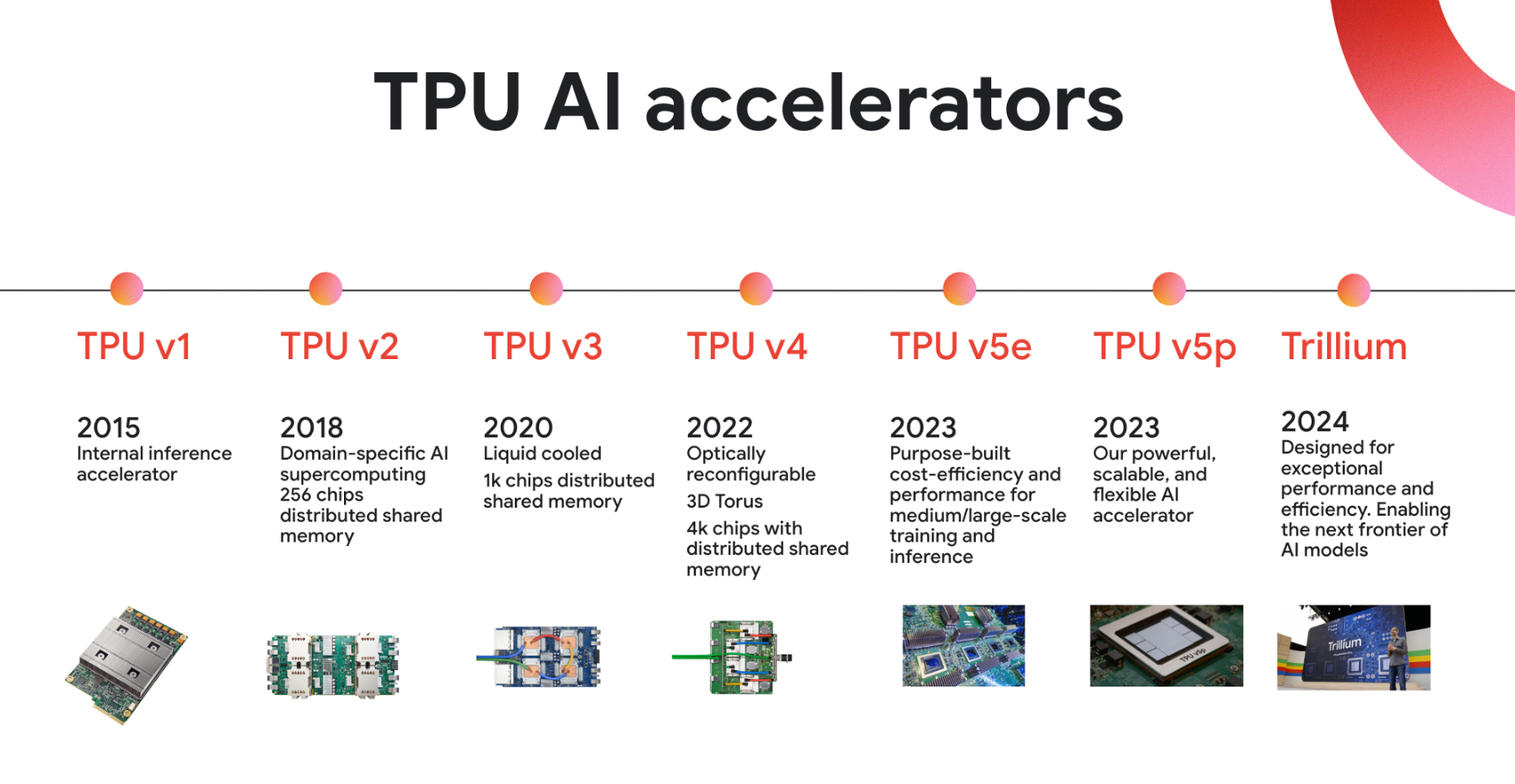
Our first such chip, TPU v1, was deployed internally in 2015 and was instantly a hit across different parts of Google.
[Want to read more about our latest custom silicon chips? Go inside the development of our Axion CPUs.]
“We thought we'd maybe build under 10,000 of them,” said Andy Swing, principal engineer on our machine learning hardware systems. “We ended up building over 100,000 to support all kinds of great stuff including Ads, Search, speech projects, AlphaGo, and even some self-driving car stuff.”
In the decade since, TPUs have advanced in performance and efficiency across generations and spread to serve as the backbone for AI across nearly all of Google’s products.
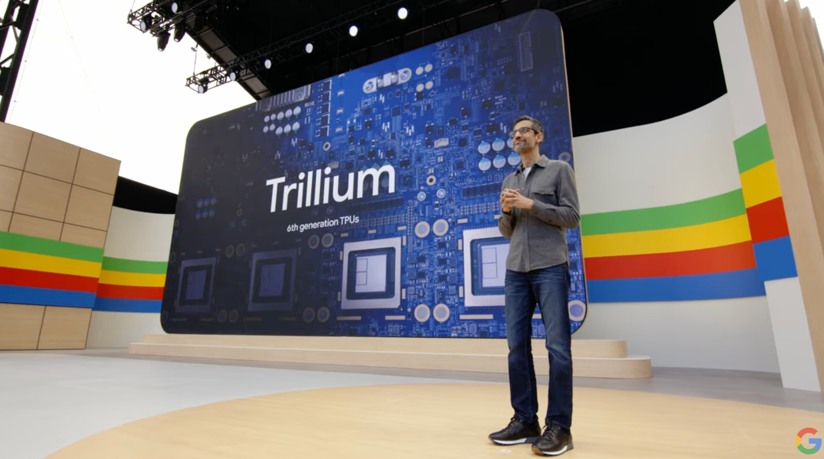
Trillium, our sixth generation TPU, offers more power and efficiency to help train our next generation of cutting-edge AI models.
And this year at I/O, we announced our next-generation TPU — Trillium, which unlocks new capabilities that we could barely have imagined when our first TPU v1 chips turned on a decade ago.
TPUs also underpin Google DeepMind’s cutting-edge foundation models, including the newly unveiled Gemini 1.5 Flash, Imagen 3, and Gemma 2, propelling advancements in AI. Trillium TPUs deliver more than 4.7x improvement in compute performance per chip (compared to the previous generation, TPU v5e) to help us keep pace with demands of even more advanced AI systems.
Keeping up with AI innovation
The evolution of our TPUs has closely matched our innovations in machine learning and AI. TPU v1 was focused on inference — helping models actually do tasks faster. But soon it wasn’t enough to just have infrastructure to run AI models quickly; we needed to be able to train new models more efficiently, too.
“In late 2014, when TPU v1 was being fabbed, we realized training capability was the limiting factor to producing models,” Norm Jouppi, VP and engineering fellow, said. “People thought a training chip would be too complicated to build… so we decided to build a training supercomputer, instead.”
That training supercomputer was TPU v2, which took the focused hardware approach of our original TPU chips and expanded it to a much larger supercomputing system. “A big focus of ours was not just the affordability of building something to do training but also to get the scale. So we built an interconnected machine — our first TPU pod — with 256 TPU chips connected with a very high-bandwidth, custom interconnect to really get a lot of horsepower behind training models,” Swing said.
A key goal for TPU v2 (and our subsequent hardware generations) was balancing between specializing our silicon design for training and serving contemporary models while still staying flexible enough for rapid change. “We didn’t know what models would look like in 2–8 years, but we know they will be based on tensor math,” Jouppi said. “So it was better to give up the last 10–20% of optimization in order not to overspecialize the accelerator and make it obsolete after a year.”
Since then, we’ve released new TPU chips and systems on a faster and faster cadence, expanding the size of our TPU pods to contain more and more chips and making further leaps in performance, efficiency, and processing power. The technology that goes into TPUs has become more complex: for example, liquid cooling was added with TPU v3 to help address efficiency needs, while TPU v4 introduced optical circuit switches to allow the chips in pods to communicate even faster and more reliably. And as it has, it’s brought new challenges.
“For example, in TPU v2 or TPU v3, we didn’t have to worry too much about the bend radius on the cables that connect each chip together,” Swing said. “But with the latest generation, if you don't route the cables just right, they don't work anymore, because the data they handle is going so fast.”
Sharing the love
Google wasn't alone in looking for better ways to develop and run AI models in those early years.
“I co-founded an ML startup in 2012, and to get the compute power we needed at low cost, my co-founder would buy used gaming GPUs online and build servers on our coffee table — we’d run the GPUs and then turn on the microwave and the power would go out,” said Zak Stone, who founded the Cloud TPU program once he joined Google. “So when I came to Google in 2016, just after the first TPU was revealed at I/O, I knew we had to find a way to offer TPUs as infrastructure in Google Cloud.”
By early 2018, a small team launched the first generation of Cloud TPUs to help Google Cloud customers accelerate their own training and inference workloads. Today, Anthropic, Midjourney, Salesforce, and other well-known AI teams use Cloud TPUs intensively. Overall, more than 60% of funded generative AI startups and nearly 90% of gen AI unicorns use Google Cloud’s AI infrastructure, including Cloud TPUs.
All that processing power is still just the beginning.
“Where we landed with TPUs and the pod setup made the most sense for what our data centers were capable of at that time, but now we're changing our data center designs to match the needs even better. So the solution that’s lined up today is very different from the solution tomorrow,” Swing said. “Forget about a single chip, or a single TPU pod — we’re building a global network of data centers filled with TPUs. The future is full stack customization all the way, from silicon to concrete.”
