Google Cloud and Dell PowerScale transform semiconductor design models
Guy Rinkevich
Principal Architect, Google Cloud
Bala Rajendran
Global CTO, EDA and Semiconductor, Dell
New technologies like integrated artificial intelligence (AI), edge computing, 5G communications, and Internet of Things (IoT) products, as well as the emergence of customers as competitors with in-house chip design capabilities are forcing the semiconductor industry to shift away from a focus on engineering and operations and toward a strong focus on product development, new operating models, and new market penetration.
According to a 2021 Semiconductor Transformation Study (STS) from Deloitte Consulting and Global Semiconductor Alliance (GSA), 42% of semiconductor companies are experimenting with new go-to-market strategies such as selling integrated solutions and experimenting with nontraditional, cloud-based business models. This is changing the way semiconductor companies go to market, engineer products, and generate revenue.
Semiconductor Integrated Circuit (IC) design, also commonly known under an umbrella term EDA, encompasses many workflows that are used to design a circuit (or “chip”). These design workloads are compute and storage centric, requiring large quantities of high-performance compute, and scalable Network Attached Storage (NAS) storage systems for the design of chips. Bringing a chip design as a finished product to the market quickly is crucial for EDA companies, and hence, faster and agile compute and storage infrastructure are essential for the design teams. With increasing design densities, moving from seven to three nanometer, the chip designs are becoming more complex and the demand for highly scalable and performant storage and compute capabilities are ever increasing.
Dell PowerScale for Google Cloud
Google and Dell make it easier to run electronic design automation (EDA) workloads in the cloud, providing a foundation for semiconductor companies to scale their clients and jobs easily while still retaining the same shared volume across all clients, with a high performance and low latency service. The solution provides a tightly integrated, self-service, multiprotocol, file service offering in Google Cloud.
Dell PowerScale is tightly integrated with Google Cloud and delivers many benefits including:
Scale-out storage that grows linearly as thousands of EDA simulation jobs (e.g., simulation) are running concurrently
On-demand dedicated capacity to achieve faster aggregate run times, flattening the design curve
Flexible architecture supporting engineers and developers the ability to run workflows in the cloud or on-prem without re-platforming apps or learning new tools
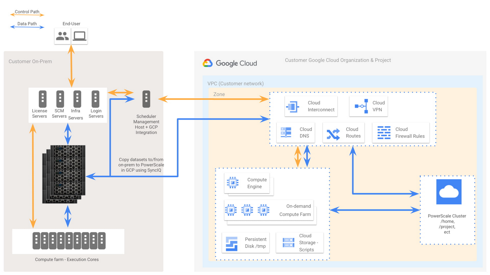
Architecture Overview; Burst to cloud chip design
Front-end workflows such as verification and synthesis are compute intensive (some tools are storage I/O intensive too) and the associated jobs tend to be short-lived. Availability of a large number of compute slots for the duration of the job is very valuable to design teams. This requirement is amplified when dealing with larger portions of designs or complex designs to be delivered in tight timelines. This is where the combined capabilities of Google Cloud and PowerScale provide the elasticity for the IC design stakeholders.
First the user interacts with their primary on-prem resources and launches a job with the scheduler directly into the Google Cloud.
The necessary compute instances are created on-demand based on the pre-configured or standard images, and once the resources are idle or jobs complete, they can be terminated. The data sets desired for job execution can be replicated ahead of time using built-in PowerScale SyncIQ feature, and this can be orchestrated as well.
When the instances are terminated, the data persists, and can be reverse-replicated back to on-prem, if needed. This way, there is a bi-directional data-flow that can be orchestrated to be triggered with the jobs or managed separately.
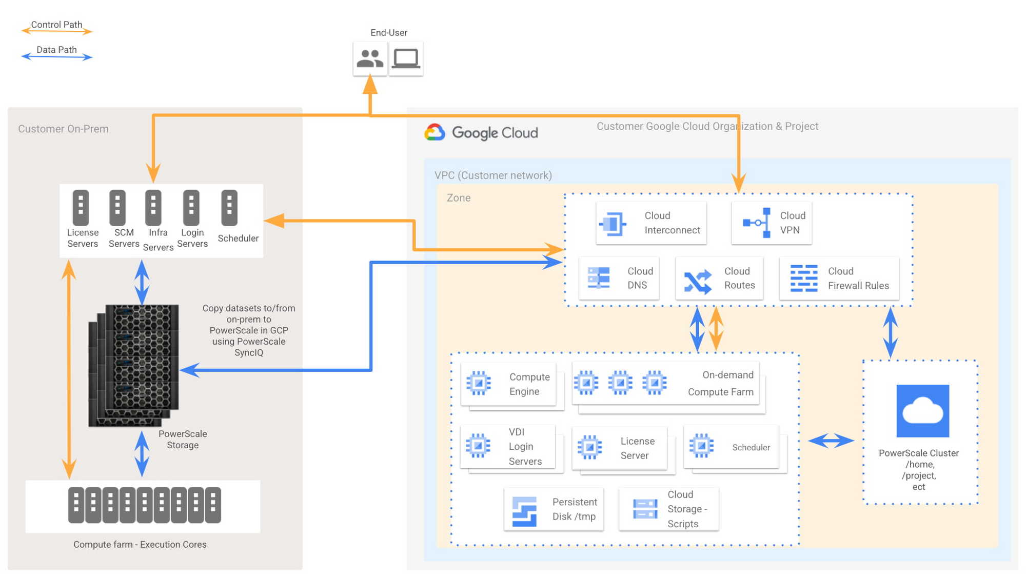
Architecture Overview: Hybrid Model
While the burst to cloud use case entails specific workflows extending into the Google Cloud, a hybrid solution can benefit a broader set of workloads. End users can interact and work directly in Google Cloud, utilizing infrastructure services and accessing datasets with no data egress just as they would for another on-prem location. Figure 2 shows that the license server can be optionally hosted in Google Cloud, or the existing on-prem server can be part of the workflow, depending on licensing requirements for various tools. The PowerScale cluster would host user homes, projects, scratch, tools, repositories and other datasets.
Linear Storage Scalability is Crucial
Selecting a storage solution that scales to meet the demand of compute workers is crucial to a successful EDA run and flattening the design curve. We tested PowerScale using a synthetic EDA benchmark suite. The test suite is used to measure the maximum sustainable throughput that a storage solution can deliver for a specific EDA workload, constructed from Back-End and Front-End subcomponents. We’ve used a Tier_1 all-flash PowerScale solution with 170TB storage capacity and 40 Google Compute Engine instances to run the tests.
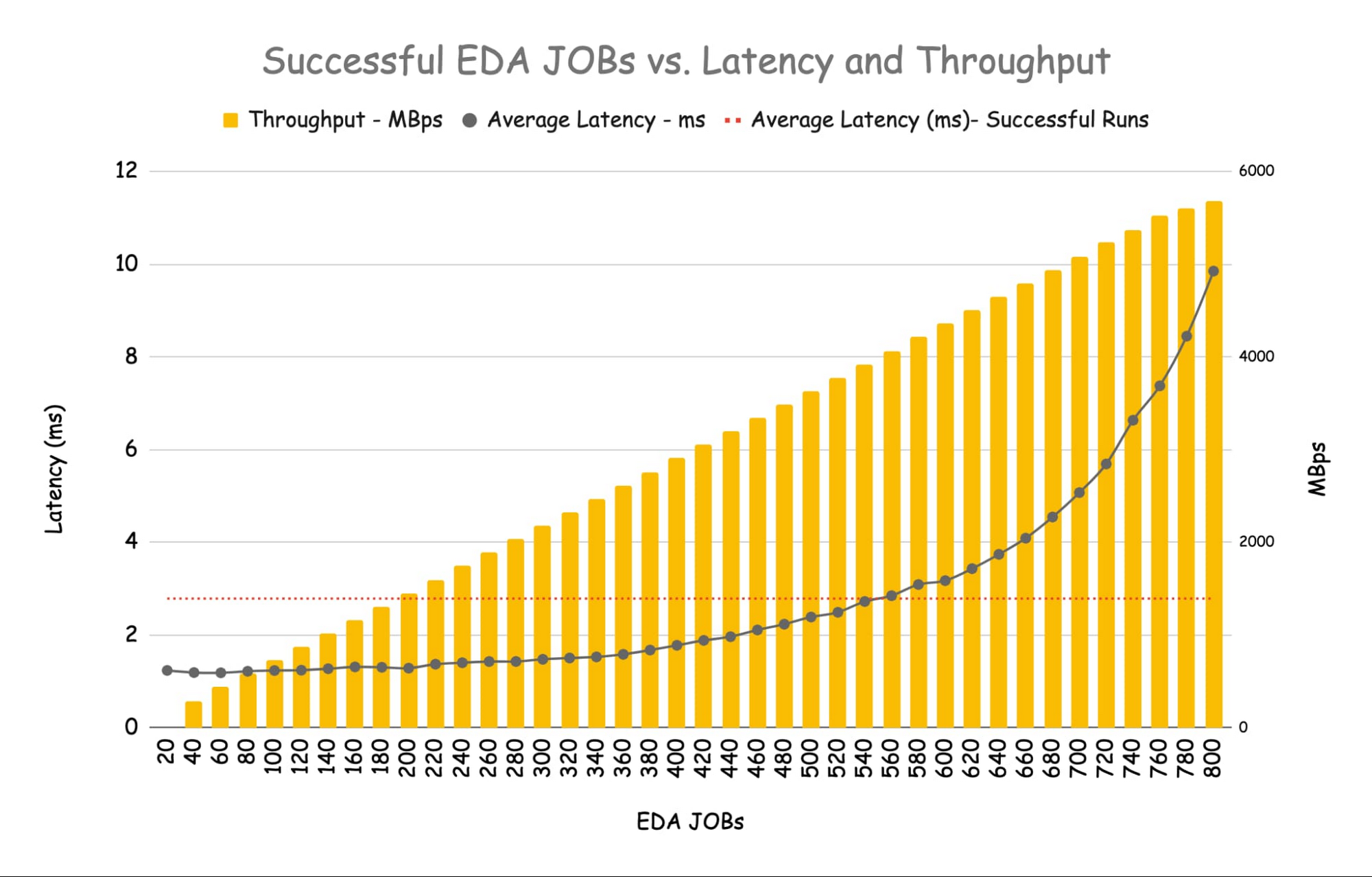
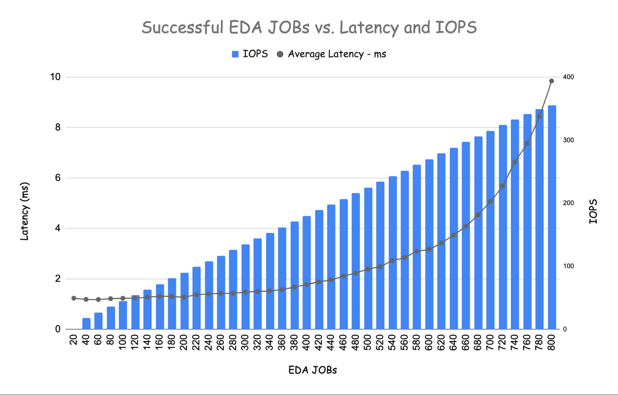
The results of the benchmark test show that with PowerScale, as you run more jobs you can deliver more throughput and IOPS. The scale-out architecture allows you to continually manage latency by adding additional nodes. This capability is critical for EDA workloads when they burst to cloud.
Additional information
Top Reasons to choose Dell EMC PowerScale for Google Cloud for semiconductor design
View webcast: Applying artificial intelligence to design verification
Read the eBook: Shaping the future of semiconductor design and manufacturing
Learn more about Dell EMC PowerScale for semiconductor design and manufacturing
A special thanks to Alec Shnapir and Sean Derrington from Google Cloud and Kami Periman from Dell for their contributions.