An in-depth look at Google’s first Tensor Processing Unit (TPU)
Kaz Sato
Developer Advocate, Google Cloud
Cliff Young
Software Engineer, Google Brain
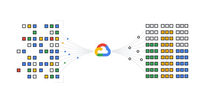
There’s a common thread that connects Google services such as Google Search, Street View, Google Photos and Google Translate: they all use Google’s Tensor Processing Unit, or TPU, to accelerate their neural network computations behind the scenes.
We announced the TPU last year and recently followed up with a detailed study of its performance and architecture. In short, we found that the TPU delivered 15–30X higher performance and 30–80X higher performance-per-watt than contemporary CPUs and GPUs. These advantages help many of Google’s services run state-of-the-art neural networks at scale and at an affordable cost. In this post, we’ll take an in-depth look at the technology inside the Google TPU and discuss how it delivers such outstanding performance.
The road to TPUs
Although Google considered building an Application-Specific Integrated Circuit (ASIC) for neural networks as early as 2006, the situation became urgent in 2013. That’s when we realized that the fast-growing computational demands of neural networks could require us to double the number of data centers we operate.Usually, ASIC development takes several years. In the case of the TPU, however, we designed, verified, built and deployed the processor to our data centers in just 15 months. Norm Jouppi, the tech lead for the TPU project (also one of the principal architects of the MIPS processor) described the sprint this way:
We did a very fast chip design. It was really quite remarkable. We started shipping the first silicon with no bug fixes or mask changes. Considering we were hiring the team as we were building the chip, then hiring RTL (circuitry design) people and rushing to hire design verification people, it was hectic.
(from First in-depth look at Google's TPU architecture, The Next Platform)
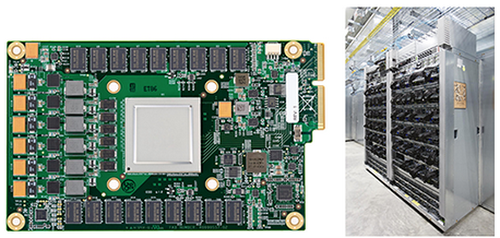
The TPU ASIC is built on a 28nm process, runs at 700MHz and consumes 40W when running. Because we needed to deploy the TPU to Google's existing servers as fast as possible, we chose to package the processor as an external accelerator card that fits into an SATA hard disk slot for drop-in installation. The TPU is connected to its host via a PCIe Gen3 x16 bus that provides 12.5GB/s of effective bandwidth.
Prediction with neural networks
To understand why we designed TPUs the way we did, let's look at calculations involved in running a simple neural network.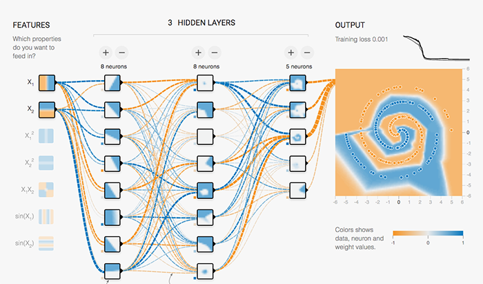
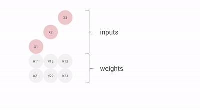
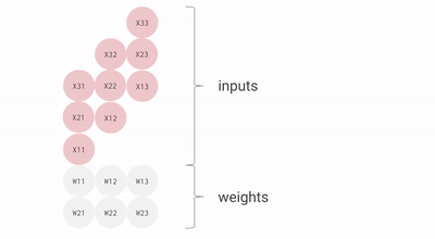
This example on the TensorFlow Playground trains a neural network to classify a data point as blue or orange based on a training dataset. (See this post to learn more about this example.) The process of running a trained neural network to classify data with labels or estimate some missing or future values is called inference. For inference, each neuron in a neural network does the following calculations:
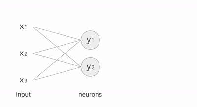
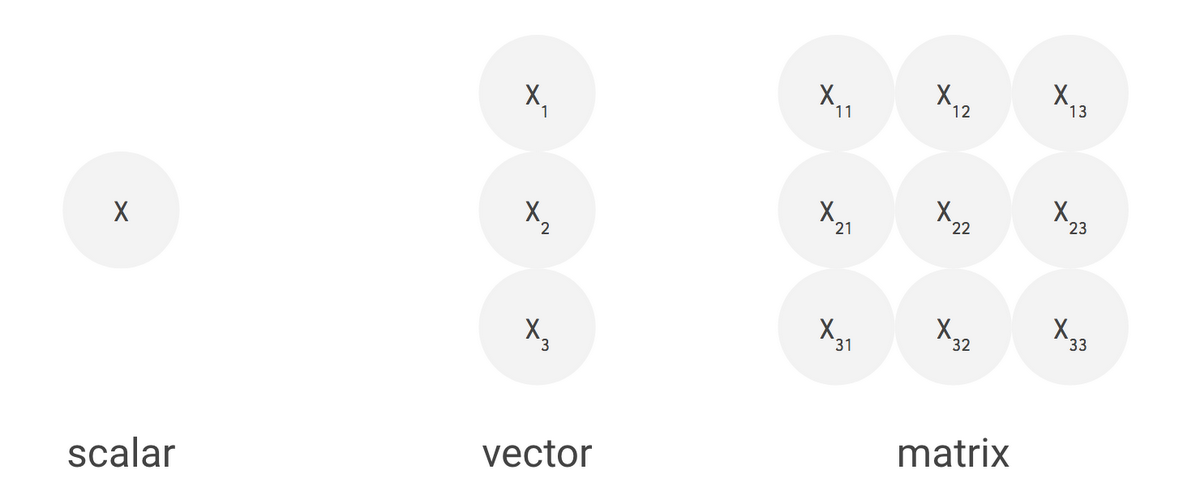
For example, if you have three inputs and two neurons with a fully connected single-layer neural network, you have to execute six multiplications between the weights and inputs and add up the multiplications in two groups of three. This sequence of multiplications and additions can be written as a matrix multiplication. The outputs of this matrix multiplication are then processed further by an activation function. Even when working with much more complex neural network model architectures, multiplying matrices is often the most computationally intensive part of running a trained model.
How many multiplication operations would you need at production scale? In July 2016, we surveyed six representative neural network applications across Google’s production services and summed up the total number of weights in each neural network architecture. You can see the results in the table below.
| Type of network | # of network layers | # of weights | % of deployed |
| MLP0 | 5 | 20M | 61% |
| MLP1 | 4 | 5M | |
| LSTM0 | 58 | 52M | 29% |
| LSTM1 | 56 | 34M | |
| CNN0 | 16 | 8M | 5% |
| CNN1 | 89 | 100M |
(MLP: Multi Layer Perceptron, LSTM: Long Short-Term Memory, CNN: Convolutional Neural Network)
As you can see in the table, the number of weights in each neural network varies from 5 million to 100 million. Every single prediction requires many steps of multiplying processed input data by a weight matrix and applying an activation function.
In total, this is a massive amount of computation. As a first optimization, rather than executing all of these mathematical operations with ordinary 32-bit or 16-bit floating point operations on CPUs or GPUs, we apply a technique called quantization that allows us to work with integer operations instead. This enables us to reduce the total amount of memory and computing resources required to make useful predictions with our neural network models.
Quantization in neural networks
If it’s raining outside, you probably don’t need to know exactly how many droplets of water are falling per second — you just wonder whether it’s raining lightly or heavily. Similarly, neural network predictions often don't require the precision of floating point calculations with 32-bit or even 16-bit numbers. With some effort, you may be able to use 8-bit integers to calculate a neural network prediction and still maintain the appropriate level of accuracy.Quantization is an optimization technique that uses an 8-bit integer to approximate an arbitrary value between a preset minimum and a maximum value. For more details, see How to Quantize Neural Networks with TensorFlow.
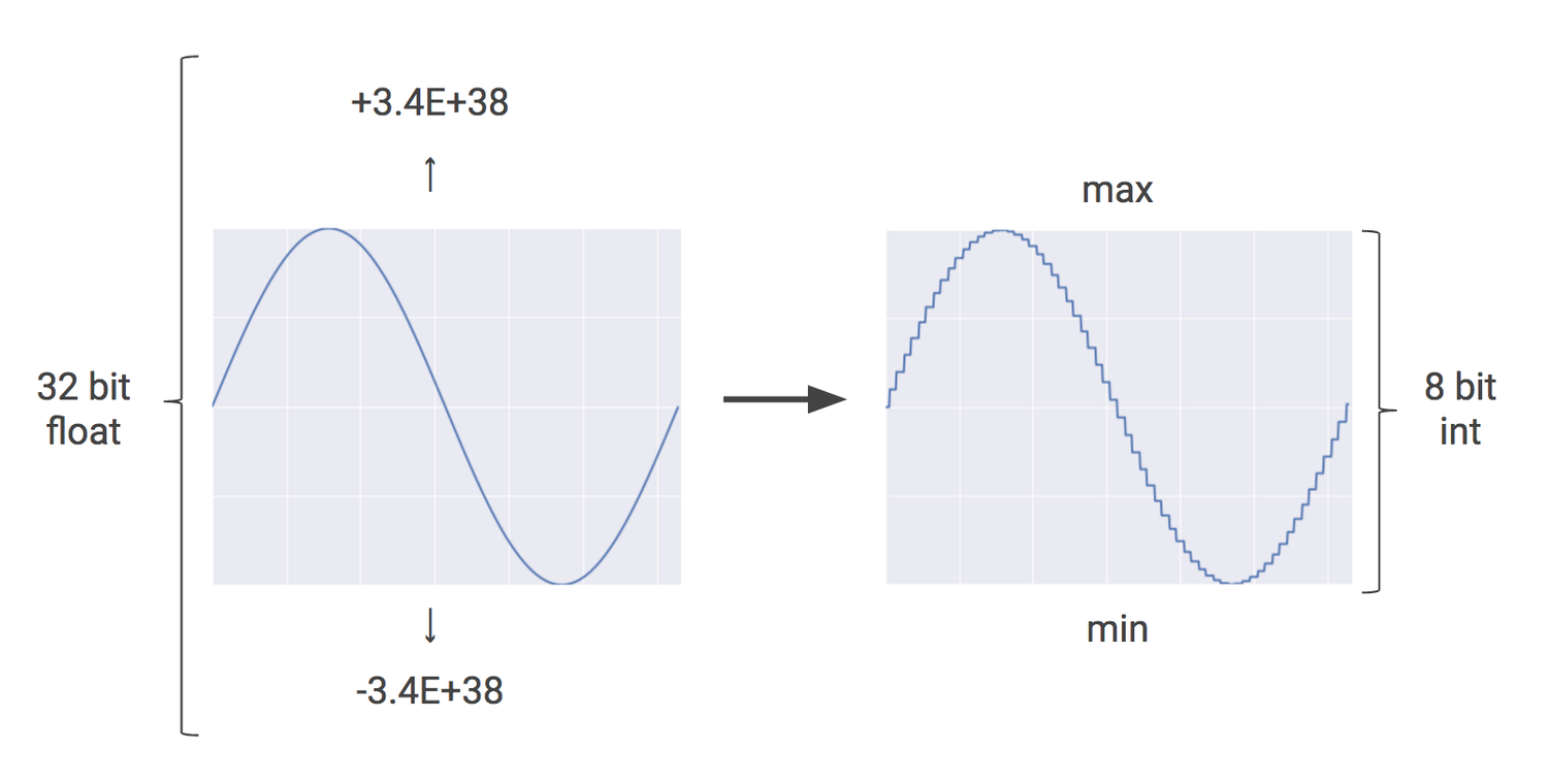
Quantization is a powerful tool for reducing the cost of neural network predictions, and the corresponding reductions in memory usage are important as well, especially for mobile and embedded deployments. For example, when you apply quantization to Inception, the popular image recognition model, it gets compressed from 91MB to 23MB, about one-fourth the original size.
Being able to use integer rather than floating point operations greatly reduces the hardware footprint and energy consumption of our TPU. A TPU contains 65,536 8-bit integer multipliers. The popular GPUs used widely on the cloud environment contains a few thousands of 32-bit floating-point multipliers. As long as you can meet the accuracy requirements of your application with 8-bits, that can be up to 25X or more multipliers.
RISC, CISC and the TPU instruction set
Programmability was another important design goal for the TPU. The TPU is not designed to run just one type of neural network model. Instead, it's designed to be flexible enough to accelerate the computations needed to run many different kinds of neural network models.Most modern CPUs are heavily influenced by the Reduced Instruction Set Computer (RISC) design style. With RISC, the focus is to define simple instructions (e.g., load, store, add and multiply) that are commonly used by the majority of applications and then to execute those instructions as fast as possible. We chose the Complex Instruction Set Computer (CISC) style as the basis of the TPU instruction set instead. A CISC design focuses on implementing high-level instructions that run more complex tasks (such as calculating multiply-and-add many times) with each instruction. Let's take a look at the block diagram of the TPU.
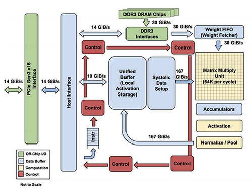
The TPU includes the following computational resources:
- Matrix Multiplier Unit (MXU): 65,536 8-bit multiply-and-add units for matrix operations
- Unified Buffer (UB): 24MB of SRAM that work as registers
- Activation Unit (AU): Hardwired activation functions
| TPU Instruction | Function |
| Read_Host_Memory | Read data from memory |
| Read_Weights | Read weights from memory |
| MatrixMultiply/Convolve | Multiply or convolve with the data and weights,accumulate the results |
| Activate | Apply activation functions |
| Write_Host_Memory | Write result to memory |
This instruction set focuses on the major mathematical operations required for neural network inference that we mentioned earlier: execute a matrix multiply between input data and weights and apply an activation function.
Norm says:
Neural network models consist of matrix multiplies of various sizes — that’s what forms a fully connected layer, or in a CNN, it tends to be smaller matrix multiplies. This architecture is about doing those things — when you’ve accumulated all the partial sums and are outputting from the accumulators, everything goes through this activation pipeline. The nonlinearity is what makes it a neural network even if it’s mostly linear algebra.”(from First in-depth look at Google's TPU architecture, the Next Platform)
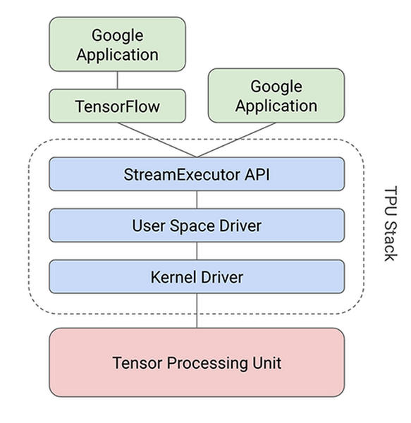
In short, the TPU design encapsulates the essence of neural network calculation, and can be programmed for a wide variety of neural network models. To program it, we created a compiler and software stack that translates API calls from TensorFlow graphs into TPU instructions.
Parallel Processing on the Matrix Multiplier Unit
Typical RISC processors provide instructions for simple calculations such as multiplying or adding numbers. These are so-called scalar processors, as they process a single operation (= scalar operation) with each instruction.Even though CPUs run at clock speeds in the gigahertz range, it can still take a long time to execute large matrix operations via a sequence of scalar operations. One effective and well-known way to improve the performance of such large matrix operations is through vector processing, where the same operation is performed concurrently across a large number of data elements at the same time. CPUs incorporate instruction set extensions such as SSE and AVX that express such vector operations. The streaming multiprocessors (SMs) of GPUs are effectively vector processors, with many such SMs on a single GPU die. Machines with vector processing support can process hundreds to thousands of operations in a single clock cycle.
In the case of the TPU, Google designed its MXU as a matrix processor that processes hundreds of thousands of operations (= matrix operation) in a single clock cycle. Think of it like printing documents one character at a time, one line at a time and a page at a time.
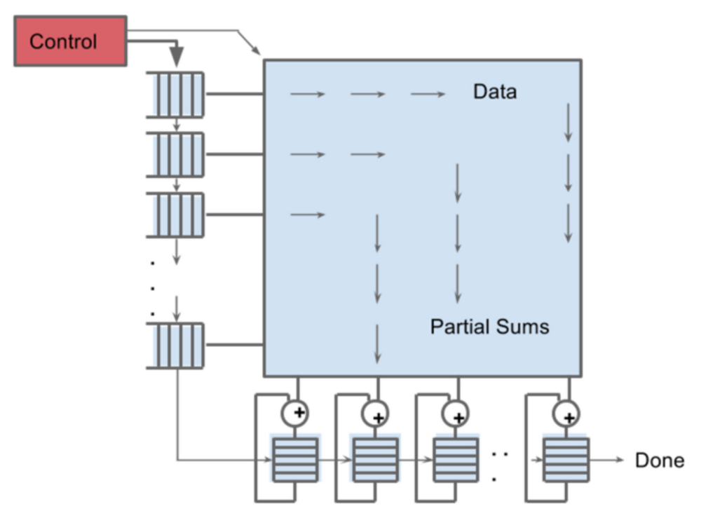
The heart of the TPU: A systolic array
To implement such a large-scale matrix processor, the MXU features a drastically different architecture than typical CPUs and GPUs, called a systolic array. CPUs are designed to run almost any calculation; they're general-purpose computers. To implement this generality, CPUs store values in registers, and a program tells the Arithmetic Logic Units (ALUs) which registers to read, the operation to perform (such as an addition, multiplication or logical AND) and the register into which to put the result. A program consists of a sequence of these read/operate/write operations. All of these features that support generality (registers, ALUs and programmed control) have costs in terms of power and chip area.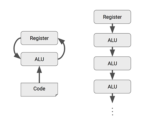
For an MXU, however, matrix multiplication reuses both inputs many times as part of producing the output. We can read each input value once, but use it for many different operations without storing it back to a register. Wires only connect spatially adjacent ALUs, which makes them short and energy-efficient. The ALUs perform only multiplications and additions in fixed patterns, which simplifies their design.
The design is called systolic because the data flows through the chip in waves, reminiscent of the way that the heart pumps blood. The particular kind of systolic array in the MXU is optimized for power and area efficiency in performing matrix multiplications, and is not well suited for general-purpose computation. It makes an engineering tradeoff: limiting registers, control and operational flexibility in exchange for efficiency and much higher operation density.
The TPU Matrix Multiplication Unit has a systolic array mechanism that contains 256 × 256 = total 65,536 ALUs. That means a TPU can process 65,536 multiply-and-adds for 8-bit integers every cycle. Because a TPU runs at 700MHz, a TPU can compute 65,536 × 700,000,000 = 46 × 1012 multiply-and-add operations or 92 Teraops per second (92 × 1012) in the matrix unit.
Let's compare the number of operations per cycle between CPU, GPU and TPU.
| Operations per cycle | |
| CPU | a few |
| CPU (vector extension) | tens |
| GPU | tens of thousands |
| TPU | hundreds of thousands, up to 128K |
In comparison, a typical RISC CPU without vector extensions can only execute just one or two arithmetic operations per instruction, and GPUs can execute thousands of operations per instruction. With the TPU, a single cycle of a MatrixMultiply instruction can invoke hundreds of thousands of operations.
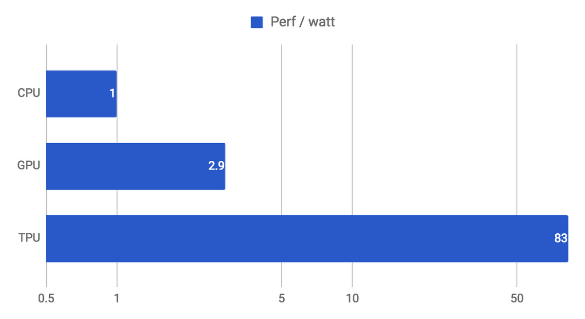
During the execution of this massive matrix multiply, all intermediate results are passed directly between 64K ALUs without any memory access, significantly reducing power consumption and increasing throughput. As a result, the CISC-based matrix processor design delivers an outstanding performance-per-watt ratio: TPU provides a 83X better ratio compared with contemporary CPUs and a 29X better ratio than contemporary GPUs.
Minimal and deterministic design
Another significant benefit of designing a new processor optimized for neural network inference is that you can be the ultimate minimalist in your design. As stated in our TPU paper:As compared to CPUs and GPUs, the single-threaded TPU has none of the sophisticated microarchitectural features that consume transistors and energy to improve the average case but not the 99th-percentile case: no caches, branch prediction, out-of-order execution, multiprocessing, speculative prefetching, address coalescing, multithreading, context switching and so forth. Minimalism is a virtue of domain-specific processors." (p.8)
Because general-purpose processors such as CPUs and GPUs must provide good performance across a wide range of applications, they have evolved myriad sophisticated, performance-oriented mechanisms. As a side effect, the behavior of those processors can be difficult to predict, which makes it hard to guarantee a certain latency limit on neural network inference. In contrast, TPU design is strictly minimal and deterministic as it has to run only one task at a time: neural network prediction. You can see its simplicity in the floor plan of the TPU die.
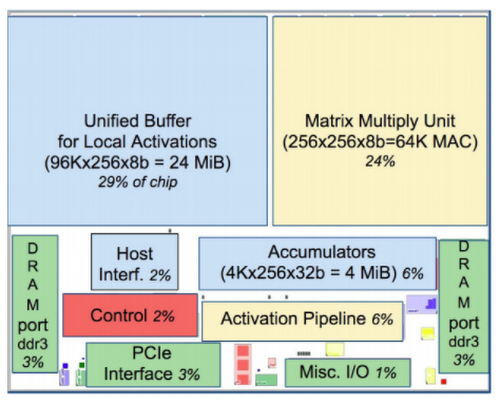
If you compare this with floor plans of CPUs and GPUs, you'll notice the red parts (control logic) are much larger (and thus more difficult to design) for CPUs and GPUs since they need to realize the complex constructs and mechanisms mentioned above. In the TPU, the control logic is minimal and takes under 2% of the die.
More importantly, despite having many more arithmetic units and large on-chip memory, the TPU chip is half the size of the other chips. Since the cost of a chip is a function of the area3 — more smaller chips per silicon wafer and higher yield for small chips since they're less likely to have manufacturing defects* — halving chip size reduces chip cost by roughly a factor of 8 (23).
With the TPU, we can easily estimate exactly how much time is required to run a neural network and make a prediction. This allows us to operate at near-peak chip throughput while maintaining a strict latency limit on almost all predictions. For example, despite a strict 7ms limit in the above-mentioned MLP0 application, the TPU delivers 15–30X more throughput than contemporary CPUs and GPUs.
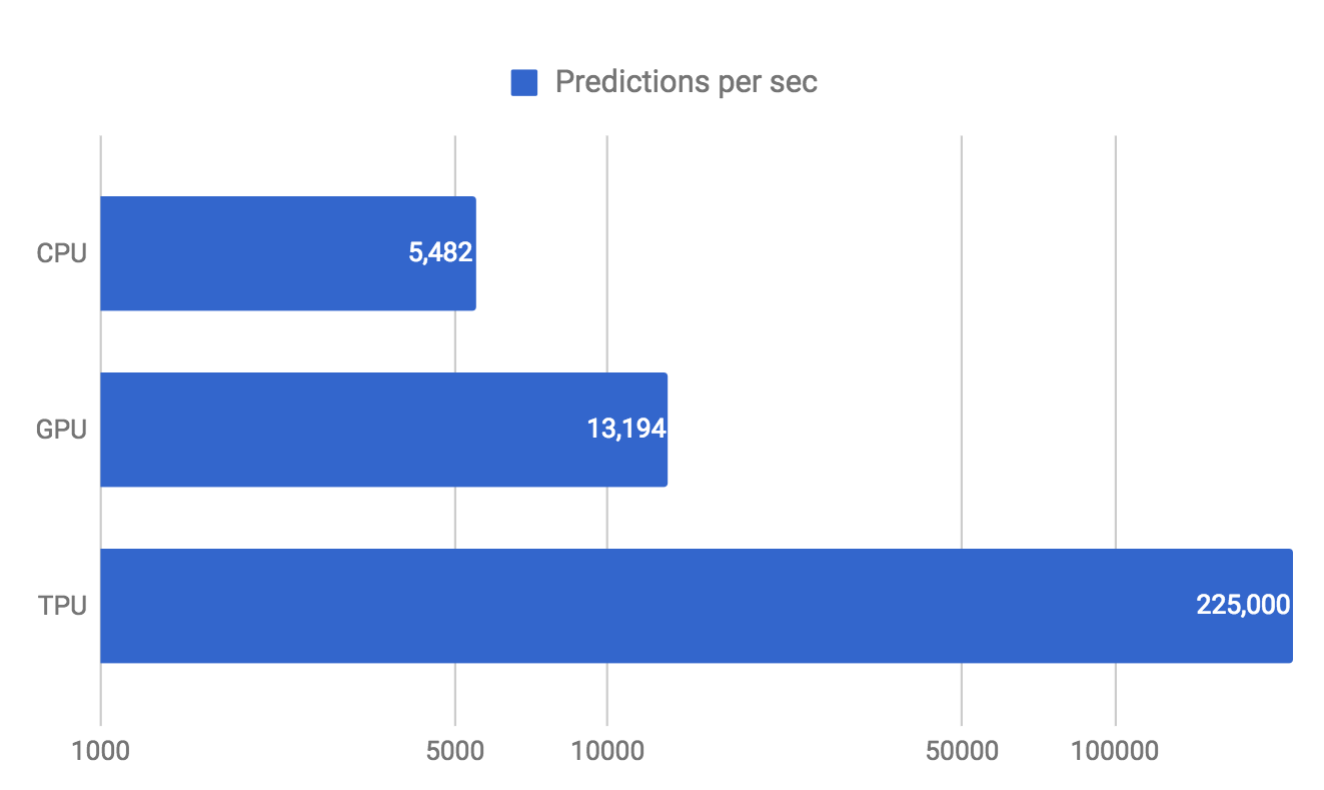
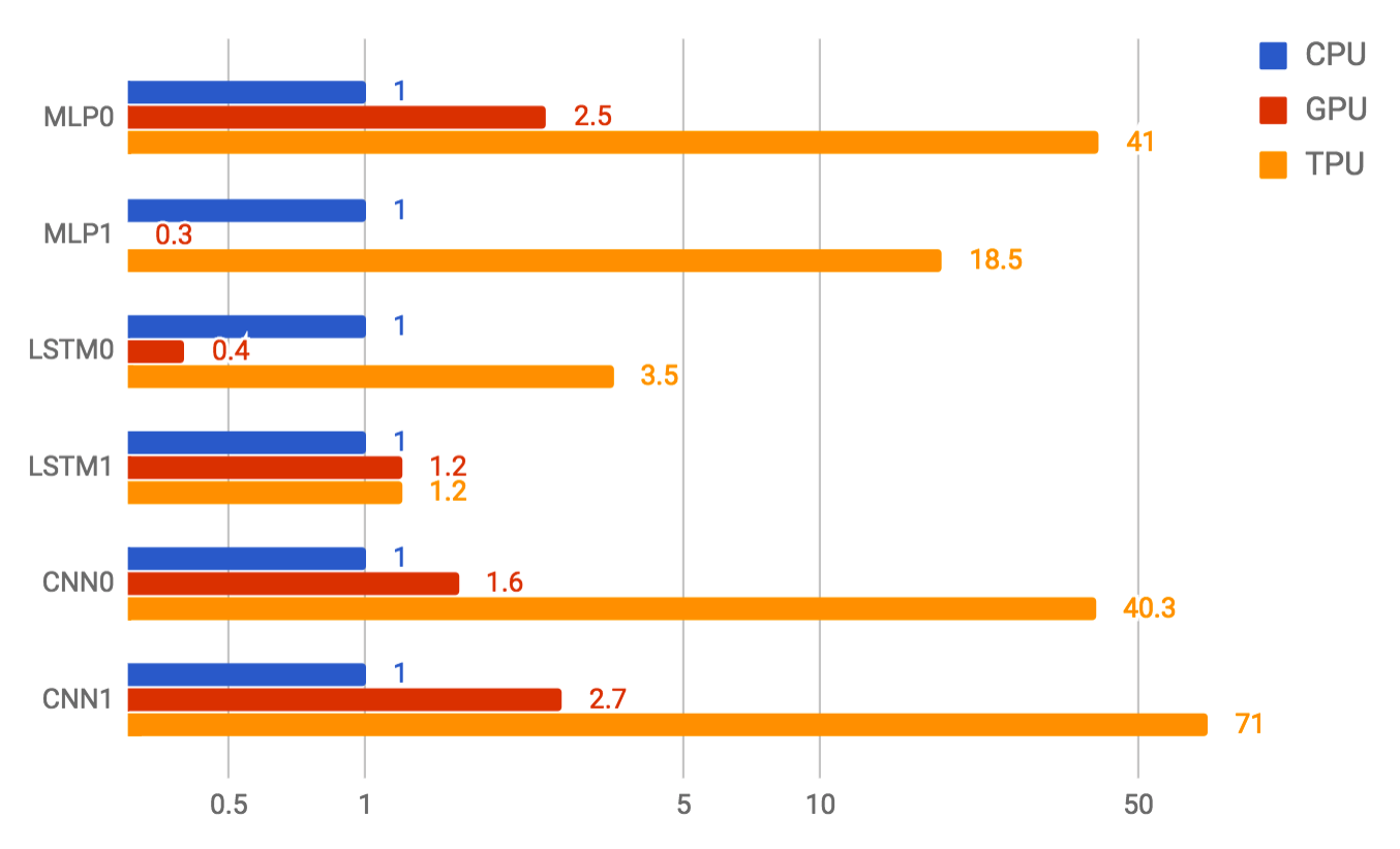
We use neural network predictions to support end-user-facing products and services, and everyone knows that users become impatient if a service takes too long to respond. Thus, for the MLP0 application, we limit the 99th-percentile prediction latency to around 7 ms, for a consistently fast user experience from TPU-based Google services. The following is an overall performance (predictions per second) comparison between the TPU and a contemporary CPU and GPU across six neural network applications under a latency limit. In the most spectacular case, the TPU provides 71X performance compared with the CPU for the CNN1 application.
Neural-specific architecture
In this article, we've seen that the secret of TPU's outstanding performance is its dedication to neural network inference. The quantization choices, CISC instruction set, matrix processor and minimal design all became possible when we decided to focus on neural network inference. Google felt confident investing in the TPU because we see that neural networks are driving a paradigm shift in computing and we expect TPUs to be an essential part of fast, smart and affordable services for years to come.Acknowledgement
Thanks to Zak Stone, Brennan Saeta, Minoru Natsutani and Alexandra Barrett for their insight and feedback on earlier drafts of this article.* Hennessy, J.L. and Patterson, D.A., 2017. Computer architecture: a quantitative approach, 6th edition, Elsevier.